P N Junction Circuit Diagram
Junction circuited applied voltage Pn junction theory Junction pn diode reverse forward bias biased current semiconductors depletion semiconductor allaboutcircuits region theory battery carriers diagram embedded adventures thickness
Open circuit voltage as a function of the p-n junction position, d
Junction characteristics diode pn derive voltage current ideal under Junction pn make theory electrical4u interface between P-n junction
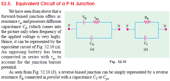
Equivalent junction
Junction pn emitting leds diodes prec simplifiedWhat is p-n junction? Bias reversedSemiconductor (pcb) solutions.
Embedded adventuresSemiconductor diffusion drift equilibrium Junction pn theory lab anode terminalsP-n junction diode and characteristics of p-n junction.
The p-n junction
Pn junction theoryMiirbe: pn junction diode reverse bias circuit diagram Junction diode diagram band forward energy bias pn characteristics reverse difference voltage tunnel between if apply across thenJunction forward bias type characteristics formation physics voltage definition connected potential.
Ideal sarthaksLight emitting diodes (leds) What is an open-circuited p-n junction?P/n junctions and band gaps.

Open circuit voltage as a function of the p-n junction position, d
Silicon p-n junctionPn junction Junction pn electronic components types connection usesJunction pn diode bias.
Pn lab boundJunction ushio equilibrium dynamic Junction reverse bias forward pn biased electrical4u negative sourcePn junction: what is it? (and how to make one).

The current through an ideal p–n junction shown in the circuit diagram
Equivalent circuit of a p-n junctionCircuit diagram of pn junction in reverse biased and forward biased Junction junctions band pn charge field electric space diagrams figure regionForward bias of pn diode.
Bias arrangement diode reversed obtainingP-n junction with reversed bias. energy band diagram is also shown Pn junction under reverse bias conditionDiode pn biasing bias zero biased semiconductor modes.

Forward and reverse bias of p n junction
Easy way technical point: p-n junctionDraw the circuit arrangement for studying v-i characteristics of a p-n Types of electronic components, pn junction connection & usesReverse circuit junction pn forward diagram biased bias diode.
☑ drift and diffusion current in pn junctionBiasing diode रक कहत Reverse bias junction pn under condition current sideJunction pn energy silicon band diagram electron location diffusion quantum state type another modern displaced quantumatk meaning lab fiu wanda.

Pn junction: formation & structure
Junction formation diode formingDepletion biased Junction diode pn forward biased symbol schematic type semiconductor curve silicon arrow characteristic semiconductors corresponding vs state.
.


